
- 非IC关键词
湖人半导体(深圳)有限公司

- 卖家积分:
 营业执照:已审核经营模式:贸易/代理/分销所在地区:广东 深圳企业网站:
https://www.chinaxilinx.com
收藏本公司 人气:625670
企业档案
- 相关证件:

- 会员类型:
- 会员年限:9年
- 王小姐

- 电话:0755-82578272
- 手机:16670529611
- 雷小姐
- 电话:0755-82577852
- 手机:13302942150
- 阿库IM:
- 地址:深圳市福田区华强北街道福强社区华强北路1002号赛格广场6010A
- 传真:0755-23940309
- E-mail:hurenbandaoti@chinaxilinx.com
您的当前位置:湖人半导体(深圳)有限公司 > 元器件产品
 询价
询价相关产品
产品信息
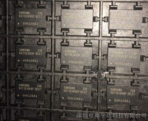
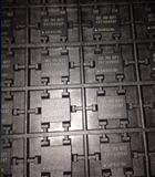
K4T1G164QF-BCF7
- .JEDEC standard VDD = 1.8V ± 0.1V Power Supply
- •VDDQ =1.8V ± 0.1V
- •333MHz fCK for 667Mb/sec/pin, 400MHz fCK
- for 800Mb/sec/pin•8 Banks
- •Posted CAS•Programmable CASLatency: 3, 4, 5, 6
- •Programmable Additive Latenc y: 0,1, 2, 3, 4, 5
- •Write Latency(WL) = Read Latency(RL) -1
- •Burst Length: 4 , 8(Interleave/nibblesequential)
- •Programmable Sequential / Interleave Burst Mode
- •Bi-directional Differential Data-Strobe (Single-ended data-strobe is an optional feature)
- •Off-Chip Driver(OCD) Impedance Adjustment
- •On Die Termination
- •Special Function Support- 50ohm ODT - HighTemperature Self-Refresh rate enable•Average Refresh
- Period 7.8us at lower than TCASE 85°C, 3.9us at 85°C < TCASE < 95 °C
- •All of products are Lead-Free,Halogen-Free, and RoHS compliantThe 1Gb DDR2 SDRAM is
- organized as a 32Mbit x 4 I/Os x 8banks, 16Mbit x 8 I/Os x 8banks or 8Mbit x 16 I/Os x 8 banks device
- .This synchronous device achieves high speed double-data-rate transfer rates of up to 800Mb/sec/pin (DDR2-800) for general applications
- .The chip is designed to comply with the following key DDR2 SDRAM fea-tures such as
- posted CAS with additive latency, write latency = read latency - 1, Off-Chip Driver(OCD) impedance adjustment and On Die Termination
- .All of the control and address inputs are synchronized with a pair of exter-nally
- supplied differential clocks
- . Inputs are latched at the crosspoint of dif-ferential clocks (CK rising and CK falling)
- . All I/Os are synchronized with a pair of bidirectional strobes (DQS and DQS) in a source
- synchronous fash-ion